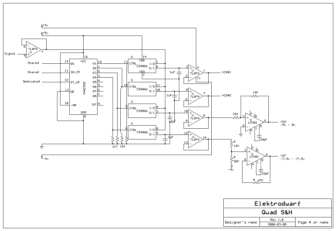
The quad sample-and-hold is intended as a replacement for multiple D/As in a digital system where more analog outputs
are wanted than avaliable D/As. The basic idea is to have a buffered voltage source that in turns charges
each of the S&Hs. Selection of which S&H to charge is done via a 74HC595 shift register which acts like
a serial data link to reduce amount of wires.
Charge and switch time depends on how much droop and how quick a signal change is acceptable/required.
I have succesfully implemented this as CV controller of multiple VCOs without any (to me) hearable drop
or "flutter" in frequency.
It's not the best s&h in the world, thinking about noise
and distortion entering the signals through mainly the 4066 switches. Also, there's a limitation to
the avaliable voltage swing; +-7.5v in the CD4066BM datasheet supplied by National
Semiconductors.
schematic
The schematic is designed for a system where the signal source generates 0-5v (5 octaves v/oct).
The output is scaled to fit 2 VCOs (0 - 5v), a VCA that decreases in CV depending on MIDI velocity (0 - -5v)
and a VCF (-7.5v - 7.5v). Op. Amps used are only due to my own convenience, the TL074's can be replaced
with any low bias-input-current Op. Amps. and the LM301 can be more or less replaced with whatever.
If having to run the logic from 5v is inconvenient, just replace the 74HC595 with a 4094.
S&H noise, distortion and droop factors can probably be much better if changing the 4066 to a more
high quality quad analog switch.
>>download schematic