
A simple, single transistor circuit can easily be incorporated onto the Model 28 Tap Clock circuit board to achieve the required signal inversion.
The schematic below depicts this circuit. Also depicted is a graphic simulation of the clock inversion where the upper trace is the input clock and the lower trace the result of the transistor inverter.
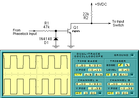
The un-modified Tap Clock advances upon the Trailing (high to low) clock edge. Most clocked devices advance upon the Leading (low to high) clock edge. The inverter depicted corrects for this, allowing Phaselock inputs to more readily synchronize.
Hardware Realization: Tim Stinchcombe has composed a step by step procedure for implementing the inverter circuit upon the Model 28 Tap Clock circuit board. This procedure reprints below. Upon review it may be noted that advanced technical skill is not required. However, thoughful approach and careful execution are required. Those not confident in these abilities might consider having someone with more experience implement this circuit modification.
|
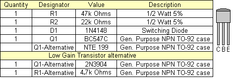
Required Components:
The invertor circuit, depicting above, requires 2 resistors, 1 diode, and 1 transistor. These are general purpose "through-hole" components easily acquired and easily used. The table right provides part number and description for these inverter components. By using the prefered high gain transistor, a relatively high value of base resistor (47k) is specified for the inverter. If the common 2N3904 is substituted for this transistor, the lower gain of this devices requires compensation by lowering the value of the base resistor. The table right summarizes this alternative. |
|
Fabrication Procedure:
The modification is made to the component side of the 'jack board', which thus needs to be removed from the module.
First gently ease off the ribbon connector which goes to the main board.
Then undo five nuts on the faceplate: the 'tap' toggle switch and the three other jack sockets in a line vertically below it, soldered to the one side of the board; the fifth nut belongs to the left-most 'accent' socket which is soldered to the other side of the board (and note that none of the nuts on the toggle switches running across the module need to be removed).
The board should now be loose, but won't quite come straight out: pull it back so the jack sockets clear the faceplate; then rotate the bottom outwards so the inner socket clears the 'switch board' running across the module, and then it can be pulled further back to completely remove it.
The remainder of the procedure depends on which revision of the jack board
is being modified: the following section gives instructions for older 'Rev
1.0' boards; for newer 'Rev 1.2' boards, see the section below.
Procedure for Rev 1.0 jack boards
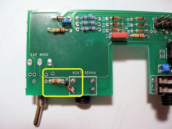
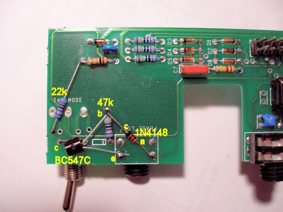
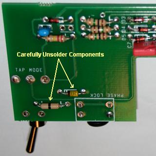
Locate the factory-fitted mod, consisting of a 1k ohm resistor and a zener diode, highlighted in the following picture:
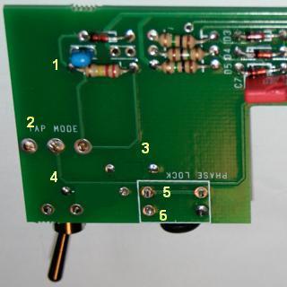
Unsolder those two components from the board. The following picture shows the board with them removed, and identifies the connection points/vias for the new components which are to be added:
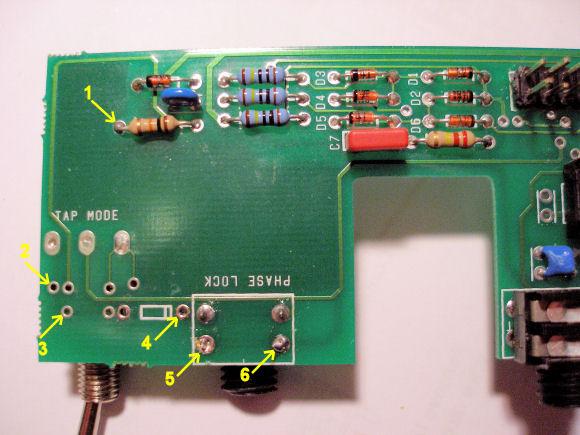
| Solder the new components onto the board as follows: | ||
| 1. | Add a 22k ohm resistor between the leg of the 10k ohm, point '1', and via '2'; when bending and cropping the leg to fit through the via, ensure that it is kept short enough so there is no chance it can touch the toggle switch on the other side of the board. | |
| 2. | Bend the leg of a 47k ohm resistor close to its body, crop it off, and solder into via '4'; bend the other leg up, away from the board. | |
| 3. | The BC547C is fitted with the flat face to the board: bend the collector under the body, and then bend the tip to fit through via '3', and solder in place (again taking care to ensure it cannot touch the toggle switch on the other side of the board); splay the base and emitter so that the emitter can be soldered to pin '5', and the base to the end of the 47k. (If a different type of transistor is used, ensure the 'c', 'b' & 'e' connections go as shown). | |
| 4. | Solder the anode end of an 1N4148 diode to pin '6', and the cathode ('black band' end) to the 47k/base connection; crop the leg of the resistor close to the solder joint. | |
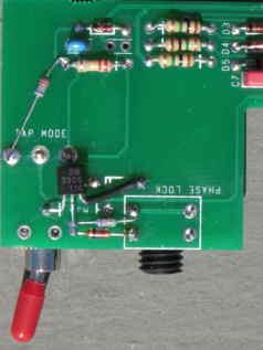
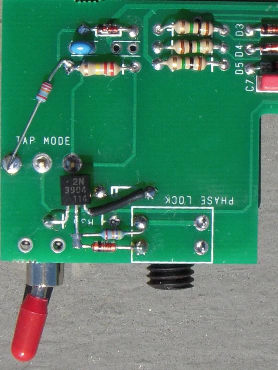
The completed mod should look something like the following picture:
Check that there are no leads touching anything they shouldn't (the vias under the collector leg of the transistor are all on the same track, so that is not a problem), and re-insert the board into the faceplate and re-attach the ribbon from the main board; replace all the nuts on the switch and the sockets, and finally double-check that none of the new leads sticking through the board can make contact with the shell of the toggle switch.
- Refering to graphic upbove left, remove both unnecessary components.
-
Refering to the graphic above middle;
- Connect the 22k Resistor between point 1 and 2.
- Carefully bend the left most (collector) and the right most lead of the transistor.
- Place a sleeve on the right most (emitter) lead and solder it to point 3,
- Solder the left most lead to Point 4
- Solder the base resistor (47k=Hi gain, 4.7k Low gain transistor) to Point 5 leaving its left lead laying upon the transistor inner (base) lead.
- Solder the right end of the 1n4148 diode to Point 6 leaving the left side lying upon the center (base) lead of the transistor.
- Solder the diode and base resistor to the transistor center lead
- cut the excess resistor and diode lead
- Inspect the finished modification for compliance with the image above right. Ā A large image can be referenced here