C128 Internal Memory Expansion -- V2Preliminary, Untested
My original scheme is improved by changing the 74LS257 to a 74HC4053 triple 2-channel mux/demux and adding quad NAND gate Z5. To very briefly explain: A decoded address from Z4 makes spdt analog switch Z3c substitute data bit D7 for D6 going into the 2nd MMU for every internal register except $D505. Further decoding by Z5c and -d causes switch Z3b to similarly substitute bit D1 for D0 going into the registers at $D508 and $D50A, correcting what I overlooked in my original scheme: Zero Page and Stack relocation.
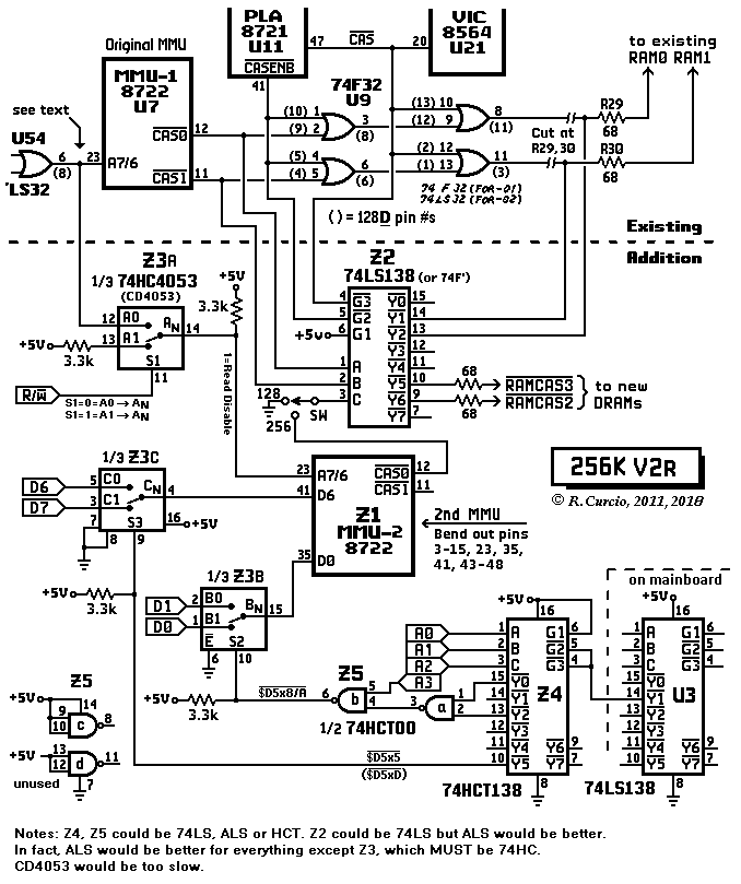 UNTESTED Switch Z3a corrects what that other internal RAM expansion overlooked: It disables reading the 2nd MMU's internal registers, eliminating the possibility of damage to one or both MMUs due to Bus Contention. Look it up. Decoder Z2 replaces the functions of U9. The two original /CASs from MMU-1 and one from MMU-2 are applied to Z2's select inputs as if they were a 3-bit "CAS code", with four of the 8 states being invalid for RAM Block selecton. Adding just two more 16-pin ICs (Z6, Z7, below,) -- plus more DRAMs, of course -- this scheme can be expanded to 512K -- but I am not recommending that! (I don't want to paraphrase the probably apocryphal statement by Bill Gates that 640K should be enough for anyone, but 256K is enough for ME, and IMO, plenty for an 8-bit computer with a top speed of 2MHz.) A better use for those two ICs would be to give 256K a mode in which Blocks0,1 and 2,3 swap places, creating in effect two 128K systems.
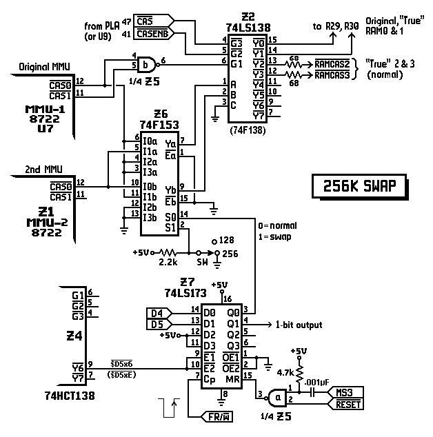 Here the values written to the presumed "SuperBank" bits of the MMU RAM Configuration Register are latched by Z7 and one of them selects normal or swapped mode. (The other bit is available for some to-be-determined purpose.) Since Z7 "parallels" the RCR the value of these two bits can be read by reading the MMU register at $D506. Another possibility is to have Blocks 2 or 3 substitute for Block1, giving a BASIC program two or three environments for variables. This would use both SuperBank bits. I haven't yet worked out the hardware details of that -- that is, how to arrange the inputs and outputs of Z6 -- and I'm pretty certain the software details dealing with multiple spaces for variables would involve more than simply changing a few pointers. I will upload more information if there is sufficient interest. email me at the address below.
|
 softhome.net