128/256/512
|
When an ingenious 256K memory expansion for the Commodore64 appeared in Transactor magazine, I began to give serious thought to doing something similar for the C128. I did not make any progress until I abandoned any thought of making it duplicate the Transactor design when in C64 mode or indeed having any additional memory available at all in C64 mode.
Besides being non-existent in C64 mode, I set other specifications for the expansion, one being that minimal changes should be made to the '128 circuit board. This I achieved: only one end of two resistors needed to be cut and new ICs were added either by sticking them upside-down to the circuit board using double-stick tape (The Dead Bug technique,) or by piggy-backing. A related requirement was that the existing Dynamic RAM ICs (or any other ICs, for that matter,) should not be removed. This was in keeping with the further requirement that the modification, while not intended for absolute beginners, be relatively easy to perform by those with some d.i.y. electronics experience. It seemed to me that desoldering sixteen 16-pin ICs (in the "flat" '128), a total of 256 pins, would give too many chances for causing damage to the C128 board in the form of broken traces or ruined feed-thru holes. The final requirements were that the modifcations should be applicable to both the slim C128 and the '128D, and that the added memory be accessible using normal Basic 7 commands and Kernal calls. This meant that only existing MMU registers were to be used to manipulate System RAM, with no new registers or latches at new I/O locations that had to be taken into account.
I had wanted my expansion to be
published in Transactor. They had been very receptive of my program
submissions. Alas, Transactor went under in the Great Magazine Shakeout
before I could work out all the details and my C256/512 expansion
appeared in TwinCities128 #30 and 31.
(Note: This page summarizes my original 256/512K expansion. For the new and improved -- but so far untested as of August, 2013 -- Rev 2.0, go HERE..)
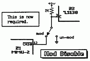
Two very complex ICs in the C128 controlled memory banking: the Programmed Logic Array and the Memory Management Unit, the latter being the more important to the task at hand. In the MMU, bits 6 and 7 of several registers determined which 64K block would be accessed. This should've allowed a total of 4 blocks, but the MMU ignored the state of bit 7, so any access of block 2 or 3, whether by Basic or the O.S. would 'wrap' to blocks 0 or 1. What's more, the MMU lacked pins for enabling the nonexistent RAM blocks. I added a second MMU by piggy-backing it to the original with several (actually, many,) pins bent out, and some logic that would swap data bits 6 and 7 when Writing to the relevant registers of that MMU. The logic also made the 2nd MMU (MMU-2) registers Write-Only, so the data with bits 6 and 7 swapped would not conflict with the non-swapped being read from MMU-1.
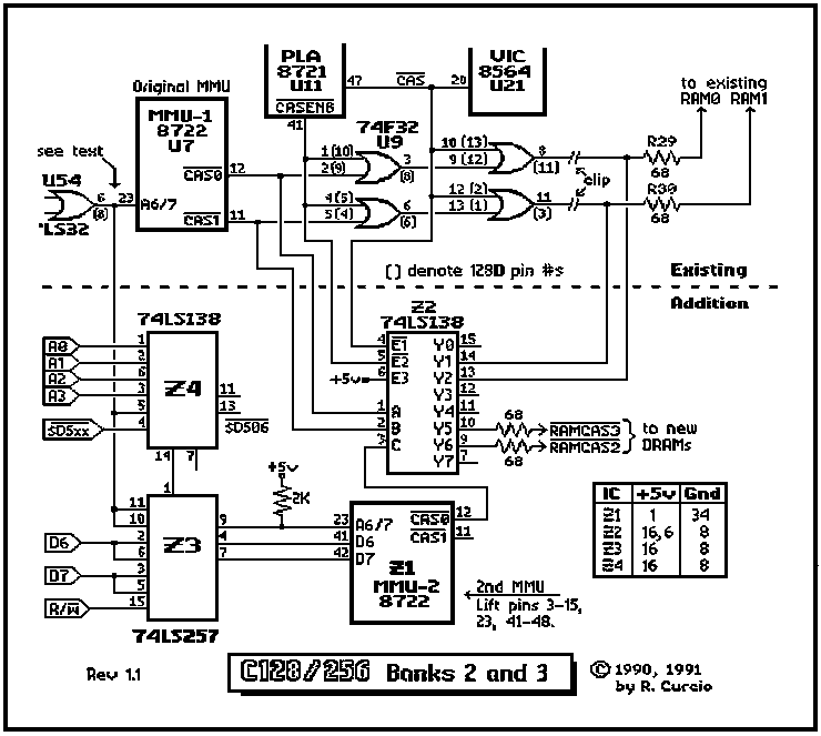 The lines labeled /CASENB from the PLA and /CAS0 and 1 from MMU(s) are enables, and the actual Column Address Strobe originates from the Video Interface Controller. After studying datasheets until I was bleary-eyed, I concluded that the speed of the 74F32 ORs that did the original /CAS steering and enabling was not necessary and a 74LS138 (Z2) would be fast enough. The combined A6/7 line on the MMU(s) is an /Enable for accessing the internal registers. When R/W is high (Read,) Z3 is disabled (pin 15 is high,) its outputs go tristate and pin 9, pulled up by the 2K resistor, makes MMU-2's registers Write-only.
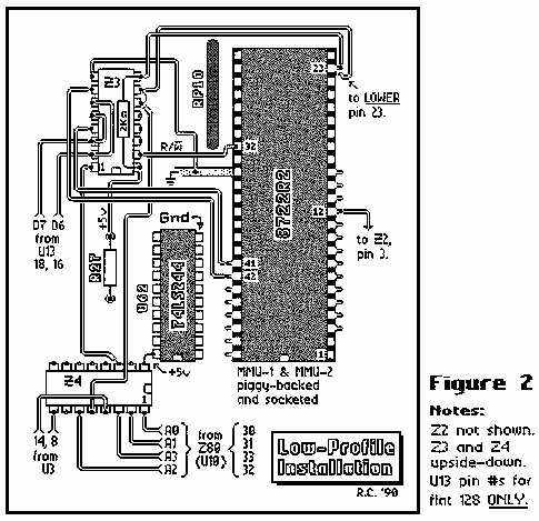 In the 'flat' C128 memory consisted of two rows of eight 64Kx1 DRAMs. For the additional memory I opted to use 64Kx4 DRAMs and piggy-back them to four of the existing 64Kx1 DRAMs for two reasons. 1] That capacity DRAM kept the CAS-enabling method of selecting banks simple, and didn't require a complicated generating of a 9th multiplexed address bit that 256Kxn DRAMs would've required. 2] Desoldering any ICs from the C128 appealed to me even less than desoldering any from the C64.
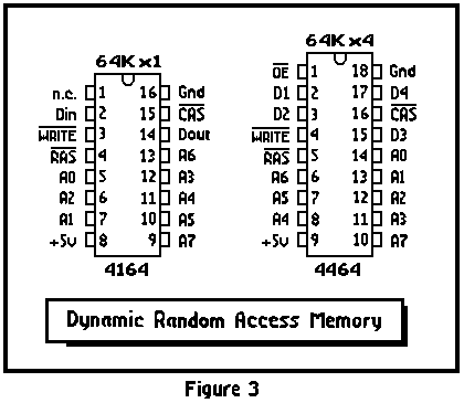 As you can see, when aligned as shown in Fig.3, most of the pin functions of the two different size packages line up. It does not matter that the 64Kx4 Address pins are in a different order than the 64Kx1.
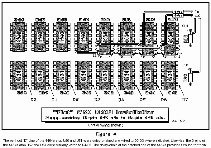 I would do this differently, now (if I were to do it at all, which is unlikely,) and put the added DRAMs on top of every other existing DRAM of the rear row; U46, U48, U50 and U52. Nearly every intermittent bug in the several modifications I performed were traced to bad soldering in the tight space between ICs. Adding DRAMs to the C128D was much easier. It used four 64Kx4s and so the piggy-backed DRAMs only needed their /CAS pins bent outward. This expansion added no new I/O locations to the machine and required no special steps to access the new memory. Issue the proper BANK statement in Basic and then PEEK, POKE, BSAVE or BLOAD the new memory to your heart's content. Perform the required setup and the O.S. routines will JSR, JMP and otherwise access the new blocks just as easily. Getting the VIC to display RAM2 or 3 as screen memory took no greater effort than it did to make it display RAM1 instead of the default RAM0. My published plans included a Basic program that did just that to demonstrate how easy it was. There was, unfortunately, one short-coming that I did not become aware of until this expansion was in the hands of others besides myself.
Famous Last Words:
One exotic and difficult to use --
one might even call it arcane -- feature of the MMU is the abilty to relocate the
8502 processor Zero Page and Stack to any page in RAM0 or any other 64K
block. I hadn't allowed for that possibility. *(I now know how to
correct that over-sight. It would require
*I have re-thought this: with a slight change to the logic, changing one IC, and adding just ONE more IC, instead of two as I had at first thought, the movable ZP & Stack problem can be fixed. I'm still not sure it would be worth doing, but information for those who might be interested is available here.
4-Mode 512KOf course I had to try expanding memory beyond 256K. Bits 4-5 of an MMU register at I/O address $D506 were unused, "reserved." Common speculation was that these were to allow a future version to select four "Super Banks" of 256K -- a total 1Meg. I considered this unlikely. Z4 in my original mod had an output corresponding to that register's location (almost as if I'd planned it), and I used that combined with R/W to 'capture' what was written to those 2 bits. With slight changes to the 256K mod, and a little more logic, I used those 2 bits to give 512K four modes: The C128 could have three sets of RAM2-3 or the 2nd 256K could be configured as a 2nd set of RAM0-3 -- sort of like having two 256K systems. Needless to say, using this mode was tricky, but not impossible. I included assembler routines to initialize the added RAM4-7 and safely switch from 'true' 256K to 'alternate' 256K. I left it to more talented programmers than I to devise a 'dual-tasking' system. As far as I know, no one took up the challenge. (It was also possible to add a variation of the new logic without adding another 256K and have a mode that would cause RAM0-1 and RAM2-3 to exchange places, like having two 128K systems -- another, smaller dual-tasking environment. I did not publish that scheme.)
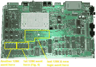 I piggybacked four more 64Kx4 DRAMS to the rear row of memory ICs -- which was not the best arrangement, since the placement of the first 4 DRAMs had proved to be a bit too cramped. Using double-stick foam tape I placed a small board with the last four 64Kx4 DRAMs and the added logic in the large open area in the center of the C128 board. A better plan would've been to use piggy-backing to place all 8 new DRAMs on the small board. In the 'flat' C128 I couldn't piggyback to the front row of DRAMs because the R.F. shield then would not fit. As it was, I had to cut an opening in the shield to accommodate the daughterboard.
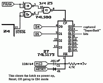 I used a quad latch because I thought the two unused latches might be handy for capturing something else. I used 3 NANDs instead a single NOR because the 4th NAND was needed by the revised bank-switching.
In retrospec, the 512K mod was
impractical, and did not integrate into Basic and the O.S. as
seamlessly as the 256K mod. (Which is why you see only the latch
portion of the schematic, and not the complete 512K mod.) But the 2-bit
latch it needed could be useful for banking of my Internal Function RAM
or some other use. With the dubious wisdom of years, I now feel that
256K is plenty for an 8-bit micro (Especially one that ambles along at
2MHz, tops!), and massive amounts of RAM is gluttonous and just plain silly. However, for the 65C816, that's a different matter.
The complete TwinCites128 256K and 512K articles can be found HERE, (with my last name misspelled on the title page) but as I've said, that version is not compatible with programs that relocate Zero Page and/or the stack. The construction details, however, are for the most part applicable to the new and improved but so far untested Version2.
|