 My first internal expansion of Vic-20 memory was straightforward, but too many parts for the amount of memory obtained. I used four 2Kx8 Static Rams and half a dual 2-to-4 decoder for 8K. I also provided Ram for the 3K "hole" in the Vic's memory map in the form of one 2Kx8 and two 1Kx4 chips. A dipswitch accessable on the right side of the case was used to select which 8K Block of Vic memory my expansion would occupy and enable/disable the 3K. There were also 'Write Protect' switches to emulate ROM.
For my next effort I wanted to decode I/O more thoroughly as well as fill as much memory space as possible. Before I could do that I had to figure out where my Vic was different from what was shown in the schematic in the back of the Programmer's Reference Guide. (If I'd had the more accurate Sam's Photo Fact Schematic sooner I'd have saved myself the trouble of tracing out the circuitry shown below.) The most important differences to me were in the Clock and Timing circuits and the internal Shared Busses. 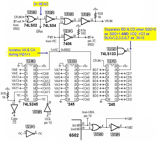 NEXT NEXT |