 Expanded I/OĀĀNEXT
The next thing I needed to do was decode the wasted I/O space. Although the Video Interface Controller and VIA ICs each contain 16 registers, due to incomplete address decoding they occupied a full 1K of I/O space, with repeating 'images.' The half 74LS139 on the left decodes that 1K space into four 256-byte pages.
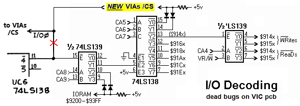 NEXT NEXTThe first page ($90xx) corresponds to the Video Controller's 'base' address. Since that chip does its own decoding of its registers, the Y0 output of the first 1/2 'LS139 is left unconnected. The next page ($91xx, '139 output Y1) is where the VIA's are located, and that is decoded by a 74LS138 into eight 32-location 'paragraphs.' The first two ('138 outputs Y0 and Y1) are diode ANDed to enable the VIAs at their base locations. (The VIA's active-high CS pins handle the rest of the decoding.) The VIAs therefor occupy 64 addresses, with fewer images. The next paragraph ($9140-$915f, output Y2) is decoded by the other 1/2 'LS139 into two pairs of /ReaD and /WRite signals, one pair ($9140-914f) for the 'Configuration Register' I planned to control my other additions. The second pair of /RD /WR at $915x is unused, for now. The five remaining 32-byte paragraphs ($916x-$91Ex, '138 outputs Y3 thru Y7) are unused, 'reserved for future expansion.' I intentionally made them each 32 locations to accommodate C64 SID chips. The last 2 pages of the original 1K space ($9200-$93ff) are diode ANDed for 512 bytes of RAM 'hidden' in the I/O area. (I'm not proud of resorting to diode logic, but I wanted to keep the chip count as low as possible.) This circuitry was added to the main board by sticking the chips to the board upside-down, and wire-wrapping to the pins. This is sometimes called the "dead bug" technique. (The logic has recently been updated to a 22V10 GAL, adding Sž1 to gate some enables.) |