
This is pretty straightfoward: an 8-bit latch and tri-state buffer with inputs and outputs wired together to form an 8-bit R/W register. System /reset clears the latch to all zeros on powerup. SŘ1 provides the proper timing for reading the buffer. I will explain the control bits on the following pages. Note that I4 of the buffer (IX5i) and Q4 of the latch (IX5o) are not tied together as the other Inputs and Outputs are. This will also be explained 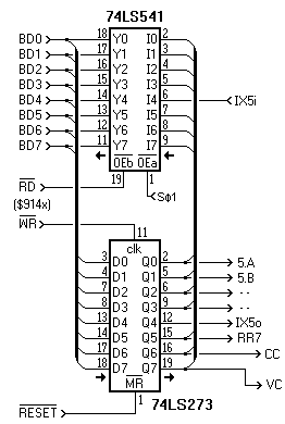 NEXT NEXT |