ĀĀBack to Projects
An Idea Whose Time Has Passed?
Fully revised 2014
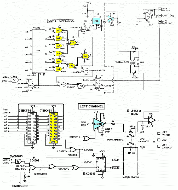
When I first saw the Oberheim digital 2-voice keyboard schematic, my reaction was, 'This looks do-able' -- because I immediately saw that the number of ICs could be reduced and the wiring simplified. (Yeah, I know...a PIC or other microcontroller could do it even simpler, but I know me: I'd get so involved with the journey I'd lose sight of the destination -- like I did 2 decades ago.)Below, for comparison, you see the "Left" channel of the original circuit and my revision. (Reduced in size and not meant to be readable enough to work from.) In the drawings which follow, I have for the most part omitted IC pin numbers, leaving that for when this gets built -- if ever. Also, most resistor and cap values are "to be determined." This is by no means a finished (re)design.
Click to view full-size Left Channel Logic
(The original schema uses '*' to designate NOT -- inversion or active low. I've used the overbar. I've also renamed CLOCK* to /STROBE because that's what it does.)In the original circuit the purpose of that cluster of 6 XORs (1 Į ICs), 4-input NOR (Į IC), 2-input NOR (╝ IC), and 2-input NAND (╝ IC) is to compare the value in the 74C174 latch with the keyboard scanning count and provide an active low at the NAND output when the two values are equal. This can be done by a single chip that didn't exist when the Ob2V was created, a 74HC688 (in yellow,) 8-bit equality detector. This reduces the number of chips and also eliminates the hassle of interconnecting all those XORs, NORs and NAND -- twice! The 74HC688 can be used in other designs that compare groups of bits. Since it compares two 8-bit values, here two P inputs and two Q inputs are held at 0, Gnd, as is the /Enable. (Curious that inputs be designated 'Q' -- that's usually reserved for flip-flops, latch and counter outputs.)
Another parts reduction is realized in the Sample and Hold, originally made with a CD4016 analog switch and an LM308. The LF398 (in pale blue,) combines all the elements needed for an S/H without the supply voltage trickery needed to make the '4016 able to handle negative voltages.
The RIGHT CHANNEL logic is the same as the LEFT, with its corresponding 'R' signals substituted for 'L.' Note that either circuit alone can function as a mono keyboard if the xTAKEN input to the 4-input NOR at the bottom left is held low. Note also that 'Left' and 'Right' do not refer to pressed key locations on the keyboard, but to which CV and Gate channel has 'First' priority as set by the MODE switch. The two channels could just as legitimately be called A&B or 1&2.
If my understanding of the logic is correct, the pulse that clocks the latch (which I've changed to a 74HC574 because its pinout makes more sense than the 74C174,) happens only when a key is first pressed, to store the scan count for comparison on suceeding scans. This can possibly be used to derive a Trigger, but the pulse would have to be stretched.
Full Left-Right Schematic
ĀĀ
Back to Projects contact: rocking softhome.net